- 您现在的位置:买卖IC网 > Sheet目录3884 > PIC16F627T-04E/SO (Microchip Technology)IC MCU FLASH 1KX14 18-SOIC
PIC16F62X
DS40300C-page 10
Preliminary
2003 Microchip Technology Inc.
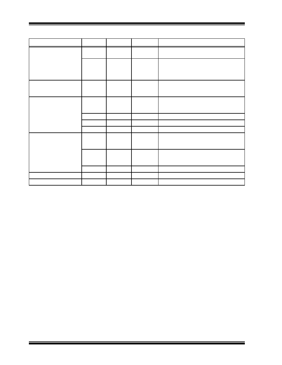
RB4/PGM
RB4
TTL
CMOS
Bi-directional I/O port. Can be software
programmed for internal weak pull-up.
PGM
ST
—
Low voltage programming input pin. Interrupt-
on-pin change. When low voltage program-
ming is enabled, the interrupt-on-pin change
and weak pull-up resistor are disabled.
RB5
TTL
CMOS
Bi-directional I/O port. Interrupt-on-pin
change. Can be software programmed for
internal weak pull-up.
RB6/T1OSO/T1CKI/PGC
RB6
TTL
CMOS
Bi-directional I/O port. Interrupt-on-pin
change. Can be software programmed for
internal weak pull-up.
T1OSO
—
XTAL
Timer1 oscillator output.
T1CKI
ST
—
Timer1 clock input.
PGC
ST
—
ICSP Programming Clock.
RB7/T1OSI/PGD
RB7
TTL
CMOS
Bi-directional I/O port. Interrupt-on-pin
change. Can be software programmed for
internal weak pull-up.
T1OSI
XTAL
—
Timer1 oscillator input. Wake-up from SLEEP
on pin change. Can be software programmed
for internal weak pull-up.
PGD
ST
CMOS
ICSP Data I/O
V
SS
V
SS
Power
—
Ground reference for logic and I/O pins
V
DD
V
DD
Power
—
Positive supply for logic and I/O pins
TABLE 2-1:
PIC16F62X PINOUT DESCRIPTION (CONTINUED)
Name
Function
Input Type Output Type
Description
Legend:
O = Output
CMOS = CMOS Output
P
= Power
— = Not used
I
= Input
ST = Schmitt Trigger Input
TTL = TTL Input
OD
= Open Drain Output
AN = Analog
发布紧急采购,3分钟左右您将得到回复。
相关PDF资料
PIC18LF448-I/L
IC PIC MCU FLASH 8KX16 44PLCC
PIC18F448-E/P
IC MCU FLASH 8KX16 W/CAN 40-DIP
PIC18F448-E/L
IC MCU FLASH 8KX16 W/CAN 44-PLCC
PIC16LF874AT-I/L
IC MCU CMOS 4K FLASH LP 44-PLCC
PIC18F252T-E/SO
IC MCU CMOS 40MHZ 16K FLSH28SOIC
PIC17C766T-33E/PT
IC MCU CMOS 33MHZ 16K EPRM80TQFP
PIC17C766T-33E/L
IC MCU CMOS 33MHZ 16K EPRM84PLCC
PIC17C766T-16E/PT
IC MCU CMOS 16MHZ 16K EPRM80TQFP
相关代理商/技术参数
PIC16F627T-04E/SS
功能描述:8位微控制器 -MCU 1.75KB 224 RAM 16I/O 4MHz ExtTemp SSOP20 RoHS:否 制造商:Silicon Labs 核心:8051 处理器系列:C8051F39x 数据总线宽度:8 bit 最大时钟频率:50 MHz 程序存储器大小:16 KB 数据 RAM 大小:1 KB 片上 ADC:Yes 工作电源电压:1.8 V to 3.6 V 工作温度范围:- 40 C to + 105 C 封装 / 箱体:QFN-20 安装风格:SMD/SMT
PIC16F627T-04I/SO
功能描述:8位微控制器 -MCU 1.75KB 224 RAM 16I/O 4MHz Ind Temp SOIC18 RoHS:否 制造商:Silicon Labs 核心:8051 处理器系列:C8051F39x 数据总线宽度:8 bit 最大时钟频率:50 MHz 程序存储器大小:16 KB 数据 RAM 大小:1 KB 片上 ADC:Yes 工作电源电压:1.8 V to 3.6 V 工作温度范围:- 40 C to + 105 C 封装 / 箱体:QFN-20 安装风格:SMD/SMT
PIC16F627T-04I/SS
功能描述:8位微控制器 -MCU 1.75KB 224 RAM 16I/O 4MHz IndTemp SSOP20 RoHS:否 制造商:Silicon Labs 核心:8051 处理器系列:C8051F39x 数据总线宽度:8 bit 最大时钟频率:50 MHz 程序存储器大小:16 KB 数据 RAM 大小:1 KB 片上 ADC:Yes 工作电源电压:1.8 V to 3.6 V 工作温度范围:- 40 C to + 105 C 封装 / 箱体:QFN-20 安装风格:SMD/SMT
PIC16F627T-20/SO
功能描述:8位微控制器 -MCU 1.75KB 224 RAM 16I/O 20MHz SOIC18 RoHS:否 制造商:Silicon Labs 核心:8051 处理器系列:C8051F39x 数据总线宽度:8 bit 最大时钟频率:50 MHz 程序存储器大小:16 KB 数据 RAM 大小:1 KB 片上 ADC:Yes 工作电源电压:1.8 V to 3.6 V 工作温度范围:- 40 C to + 105 C 封装 / 箱体:QFN-20 安装风格:SMD/SMT
PIC16F627T-20/SS
功能描述:8位微控制器 -MCU 1.75KB 224 RAM 16I/O 20MHz SSOP20 RoHS:否 制造商:Silicon Labs 核心:8051 处理器系列:C8051F39x 数据总线宽度:8 bit 最大时钟频率:50 MHz 程序存储器大小:16 KB 数据 RAM 大小:1 KB 片上 ADC:Yes 工作电源电压:1.8 V to 3.6 V 工作温度范围:- 40 C to + 105 C 封装 / 箱体:QFN-20 安装风格:SMD/SMT
PIC16F627T-20E/SO
功能描述:8位微控制器 -MCU 1.75KB 224 RAM 16I/O RoHS:否 制造商:Silicon Labs 核心:8051 处理器系列:C8051F39x 数据总线宽度:8 bit 最大时钟频率:50 MHz 程序存储器大小:16 KB 数据 RAM 大小:1 KB 片上 ADC:Yes 工作电源电压:1.8 V to 3.6 V 工作温度范围:- 40 C to + 105 C 封装 / 箱体:QFN-20 安装风格:SMD/SMT
PIC16F627T-20E/SS
功能描述:8位微控制器 -MCU 1.75KB 224 RAM 16I/O RoHS:否 制造商:Silicon Labs 核心:8051 处理器系列:C8051F39x 数据总线宽度:8 bit 最大时钟频率:50 MHz 程序存储器大小:16 KB 数据 RAM 大小:1 KB 片上 ADC:Yes 工作电源电压:1.8 V to 3.6 V 工作温度范围:- 40 C to + 105 C 封装 / 箱体:QFN-20 安装风格:SMD/SMT
PIC16F627T-20I/SO
功能描述:8位微控制器 -MCU 1.75KB 224 RAM 16I/O 20MHz IndTemp SOIC18 RoHS:否 制造商:Silicon Labs 核心:8051 处理器系列:C8051F39x 数据总线宽度:8 bit 最大时钟频率:50 MHz 程序存储器大小:16 KB 数据 RAM 大小:1 KB 片上 ADC:Yes 工作电源电压:1.8 V to 3.6 V 工作温度范围:- 40 C to + 105 C 封装 / 箱体:QFN-20 安装风格:SMD/SMT